
The ACE600003 is a deterministic, real‑time fractional‑delay engine that synthesizes a complete 21‑tap Blackman‑windowed sinc kernel directly in hardware with fixed 350‑cycle latency.
Designed for wideband, sub‑sample alignment in demanding signal‑processing pipelines, the core delivers analytical interpolation accuracy without LUTs, polynomial approximations, or multi‑phase FIR banks.
At its core is a fully unrolled mathematical pipeline: a hardware CORDIC computes the base trigonometric terms, followed by optimized scaling and 21 parallel divisions to evaluate the exact sinc response for any fractional delay in the range $\tau \in [0, 1)$.
A built‑in delta‑kernel bypass guarantees numerically stable behavior near the removable singularities of the sinc function, ensuring clean, well‑conditioned output across the entire delay domain.
The ACE600003 integrates through a simple dual‑port BRAM interface, avoiding AXI and eliminating protocol overhead. The control model is deterministic and race‑free:
The ACE600003 architecture is modular, equation‑centric, and designed for long‑term adaptability across devices, bandwidth requirements, and application domains. While the default configuration implements a 21‑tap Blackman‑windowed sinc interpolator with analytical coefficient synthesis, the core can be tailored by ACE to meet specialized performance, resource, or integration constraints.
ACE supports a range of algorithmic adaptations to match application‑specific spectral or temporal requirements:
These options allow the interpolation kernel to be shaped precisely to the customer’s signal chain and spectral budget.
For deployments where area, power, or device class impose strict constraints, ACE offers reduced‑complexity configurations:
These variants preserve deterministic timing while minimizing LUT, DSP, and BRAM usage.
The core’s equation‑driven design enables straightforward migration across FPGA families and vendors:
The architecture avoids vendor‑specific primitives wherever possible, ensuring consistent behavior and predictable timing across platforms.
For customers with non‑standard interpolation requirements, ACE can integrate:
This flexibility allows the ACE600003 to serve as a foundation for both commercial and defense‑grade signal‑processing pipelines.
The ACE600003 is designed for real‑time signal‑processing systems that require precise sub‑sample timing, wideband spectral integrity, and deterministic execution. By synthesizing analytical sinc coefficients in hardware with fixed 350‑cycle latency, the core enables high‑performance fractional‑delay correction in environments where polynomial or LUT‑based interpolators introduce unacceptable jitter, bandwidth loss, or quantization artifacts.
The ACE600003 core implements a fully analytical, wideband fractional‑delay algorithm based on the classical Blackman‑windowed sinc interpolation model. For each requested fractional delay $\tau \in [0, 1)$, the engine synthesizes a complete 21‑tap FIR kernel using the exact mathematical expression:
$$h[k] = w[k] \cdot \text{sinc}(k + \tau) = w[k] \cdot \frac{\sin\big(\pi (k + \tau)\big)}{\pi (k + \tau)}$$
where:
This formulation preserves amplitude and phase accuracy across the full Nyquist band and avoids the bandwidth collapse typical of polynomial (Farrow) or LUT‑based interpolators. The computation proceeds in three conceptual stages:
For each tap index $k \in \{-10, \dots, +10\}$, the core evaluates the exact sinc term using a single shared base trigonometric evaluation $\sin(\pi \tau)$ with alternating sign parity $(-1)^k$:
$$\text{sinc}(k + \tau) = \frac{\sin\big(\pi (k + \tau)\big)}{\pi (k + \tau)} = \frac{(-1)^k \sin(\pi \tau)}{\pi (k + \tau)}$$
This ensures mathematically correct behavior for all fractional delays, with no approximations, tables, or polynomial expansions.
Each sinc value is multiplied by the corresponding Blackman coefficient:
$$h[k] = w[k] \cdot \text{sinc}(k + \tau)$$
The Blackman window provides:
This produces a wideband, high‑fidelity interpolation kernel suitable for demanding signal‑processing applications.
Near the removable singularities at $\tau \rightarrow 0$ and $\tau \rightarrow 1$, the sinc denominator approaches zero. To guarantee numerical stability, the ACE600003 automatically engages a delta‑kernel bypass:
This ensures perfectly conditioned behavior at the edges of the delay domain, with no amplification of rounding noise. In addition, the logic has a hard clip on the maximum coefficient to $1.0$ (0x40000000), avoiding any subsequent overflow in the customer FIR in case of lack of internal precision in proximity of the edge cases threshold.
The ACE600003 generates interpolation kernels without per‑kernel normalization. This is an intentional architectural decision that preserves the deterministic timing profile and minimal resource footprint of the core. A normalization pass would require a full‑kernel reduction, a second scaling pass across all 21 taps, and additional pipeline storage—introducing data‑dependent latency and breaking the fixed 350‑cycle execution guarantee. Because the Blackman‑windowed sinc model inherently maintains bounded amplitude variation, normalization provides no meaningful improvement in wideband fractional‑delay applications.
The ACE600003 Real‑Time Wideband Sinc Interpolator is engineered for deterministic, high‑fidelity fractional‑delay synthesis with a minimal FPGA footprint. The core delivers fixed‑latency coefficient generation at $200\text{ MHz}$, enabling sub‑sample timing alignment in wideband signal‑processing pipelines without the overhead of multi‑phase FIR banks or polynomial Farrow structures.
The core is exceptionally compact for a 21‑tap analytical sinc engine (AMD UltraScale+):
The ACE600003 operates with a single performance‑critical clock domain:
DNA_PORTE2 primitive (no impact on solver timing or throughput).Post‑route timing analysis confirms all constraints are met in the $200\text{ MHz}$ domain with WNS $> 2.5\text{ ns}$ and 0 CDC violations.
The ACE600003 core is packaged as an AMD IP core. Figure 2 shows the block configuration used in its verification project.
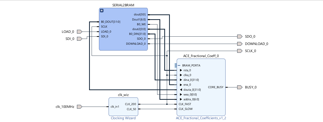
The core is managed entirely via read/write operations on a BRAM with AXI interface. The instantiated BRAM is a True Dual Port with port A available to the user and port B managed by the internal Math Engine. The BRAM has a width of 32 bits and a depth of 128 locations. The core only uses the first 80 (0 to 79) locations, with the remaining ones completely available for the user via port A.
| BRAM | ADDRESS | VARIABLE | DIR | FORMAT | DESCRIPTION |
|---|---|---|---|---|---|
| BRAM_0 | 0 | START_CMD | IN-OUT | N/A | Set to 0x1 by the user to start the computation. Set to 0x0 by the math engine at the end of computation. |
| BRAM_0 | 1 | tau_fx | IN | Fixed point 2Q30 | Fractional Delay. Possible values are between $0$ (0x00000000) and $1$ (0x40000000). |
| BRAM_0 | 2 .. 11 | w1 .. w10 | IN | FLOAT32 | Symmetric windowing function coefficients for the sinc kernel ($w_1$ through $w_{10}$). |
| BRAM_0 | 12 .. 14 | DON'T TOUCH | N/A | RESERVED | Used for internal computation storage. Changing during execution may produce unpredictable results. |
| BRAM_0 | 15 .. 24 | h_p1_fx .. h_p10_fx | OUT | Fixed point 2Q30 | Positive-index interpolation filter coefficients ($h[+1]$ through $h[+10]$). |
| BRAM_0 | 25 .. 34 | h_n10_fx .. h_n1_fx | OUT | Fixed point 2Q30 | Negative-index interpolation filter coefficients ($h[-10]$ through $h[-1]$). |
| BRAM_0 | 35 | h_0_fx | OUT | Fixed point 2Q30 | Center interpolation filter coefficient ($h[0]$). |
| BRAM_0 | 36 .. 75 | DON'T TOUCH | N/A | RESERVED | Used for internal computation storage. Changing during execution may produce unpredictable results. |
| BRAM_0 | 76 | DNA1 | OUT | BINARY | FPGA DNA [63:32] (zero-padded MSB if device DNA is shorter than 64 bits). |
| BRAM_0 | 77 | DNA2 | OUT | BINARY | FPGA DNA [31:0]. |
| BRAM_0 | 78 | USER_KEY1 | IN | BINARY | USER_KEY [63:32]. |
| BRAM_0 | 79 | USER_KEY2 | IN | BINARY | USER_KEY [31:0]. |
In addition to the BRAM interface, the core exposes:
CLK_SLOW is used for access to the DNA reader primitive (max frequency $100\text{ MHz}$, suggested frequency $50\text{ MHz}$)CLK_FAST is used to drive the internal computation engine (suggested frequency $200\text{ MHz}$)BUSY pin that, when set to high, signals when the core is executing the initialization or its main function.
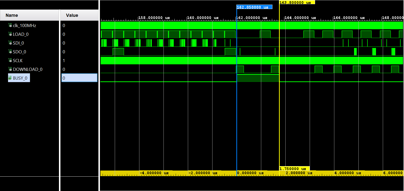
At start up, the core automatically performs an initialization that lasts (with CLK_SLOW @ $50\text{ MHz}$ and CLK_FAST @ $200\text{ MHz}$) less than $5,000\text{ ns}$. When initialization is complete, the BRAM is populated with the DNA (63 downto 0) of the FPGA (addresses 76 and 77 with MSB and LSB respectively).
Once initialization is complete, the user loads the BRAM inputs and sets START_CMD to 0x1. Results are written in BRAM after the specified 350-cycle latency, and the core clears START_CMD to 0x0 and de-asserts BUSY to 0.
Note: if the USER_KEY is not correct, the core terminates in the specified timeframe, but produces unpredictable results.
ACE600003 is delivered as a pre‑packaged Vivado IP core, ready for integration through the AMD/Xilinx IP Catalog. Each licensed core includes:
USER_KEY file for license activation
ACE provides a USER_KEY value (64 bits) bound to the FPGA Serial Number (DNA). Keys are delivered in a simple CSV file:
DNA_HEX,AUTHORIZATION_KEY
0011223344556677,C303E222F7D44C5B
ABCDE1234567890F,A2A3A3114194ED74
5566778899AABBCC,94C023F594AA6F63
DEADBEEF12345678,F40237F85DFB6F2A
00123456789ABCDE,E8ACBBDBFCF3ACB7
...............,.................BRAM_PORTA interface (addresses 76 and 77).USER_KEY from the CSV file.USER_KEY via the BRAM_PORTA interface (addresses 78 and 79).Pricing is provided directly by ACE based on deployment volume, license type, optional customization requirements, and target FPGA family.
The ACE600003 has been tested against a double-precision MATLAB golden model implementing the exact analytical equations:
function h = ACEequivalentCoefficientCalculator(tau, N)
   % ACE ANALYTICAL TAP SYNTHESIZER
   % tau : Fractional part of the delay [0, 1.0)
   % N   : Radius (e.g., 10 for 21 taps)
   % h   : Resulting filter kernel (1 x 21)

   h = zeros(1, 2*N + 1);

   % --- Stage 2 equivalent: Blackman Window Constants ---
   n_win = 0:2*N;
   % Below the suggested coefficients, the user may use different ones
   w = (0.42 - 0.5*cos(2*pi*n_win/(2*N)) + 0.08*cos(4*pi*n_win/(2*N)));

   % --- STAGE 1 equivalent: Phase Prep ---
   s_base = sin(pi * tau);
   s_base_opposite = -s_base;

   % --- STAGE 3 equivalent: Analytical Tap Synthesis ---
   for k_hw = -N:N
       arg = (k_hw + tau) * pi;
       if abs(arg) < 1e-12
           tap_val = 1.0;
       else
           if mod(k_hw, 2) == 0
               num = s_base;
           else
               num = s_base_opposite;
           end
           tap_val = num / arg;
       end

       % Apply Window Weight
       idx = k_hw + N + 1;
       h(idx) = tap_val * w(idx);
   end
end
The validation benchmark covers 30 test stages across the full fractional delay domain $\tau \in [0, 1]$:
==============================================================
  VALIDATION FOR STAGE 1 | tau: 0.000000
==============================================================
Tap Idx      | HW Float     | Golden Val   | Abs Error  | Ratio
--------------------------------------------------------------
Tap -10      |  +0.00000000 |  +0.00000000 | 0.00e+00  | N/A
Tap -9       |  +0.00000000 |  +0.00000000 | 0.00e+00  | N/A
Tap -8       |  +0.00000000 |  +0.00000000 | 0.00e+00  | N/A
Tap -7       |  +0.00000000 |  +0.00000000 | 0.00e+00  | N/A
Tap -6       |  +0.00000000 |  +0.00000000 | 0.00e+00  | N/A
Tap -5       |  +0.00000000 |  +0.00000000 | 0.00e+00  | N/A
Tap -4       |  +0.00000000 |  +0.00000000 | 0.00e+00  | N/A
Tap -3       |  +0.00000000 |  +0.00000000 | 0.00e+00  | N/A
Tap -2       |  +0.00000000 |  +0.00000000 | 0.00e+00  | N/A
Tap -1       |  +0.00000000 |  +0.00000000 | 0.00e+00  | N/A
Tap 0        |  +1.00000000 |  +1.00000000 | 0.00e+00  | 1.0000
Tap 1        |  +0.00000000 |  +0.00000000 | 0.00e+00  | N/A
Tap 2        |  +0.00000000 |  +0.00000000 | 0.00e+00  | N/A
Tap 3        |  +0.00000000 |  +0.00000000 | 0.00e+00  | N/A
Tap 4        |  +0.00000000 |  +0.00000000 | 0.00e+00  | N/A
Tap 5        |  +0.00000000 |  +0.00000000 | 0.00e+00  | N/A
Tap 6        |  +0.00000000 |  +0.00000000 | 0.00e+00  | N/A
Tap 7        |  +0.00000000 |  +0.00000000 | 0.00e+00  | N/A
Tap 8        |  +0.00000000 |  +0.00000000 | 0.00e+00  | N/A
Tap 9        |  +0.00000000 |  +0.00000000 | 0.00e+00  | N/A
Tap 10       |  +0.00000000 |  +0.00000000 | 0.00e+00  | N/A
--------------------------------------------------------------
STAGE 1 SUMMARY:  DC Gain: 1.0000000000 | Max Tap Error: 0.00e+00
==============================================================
  VALIDATION FOR STAGE 15 | tau: 0.445556
==============================================================
Tap Idx      | HW Float     | Golden Val   | Abs Error  | Ratio
--------------------------------------------------------------
Tap -10      |  +0.00000000 |  +0.00000000 | 4.56e-19  | N/A
Tap -9       |  +0.00033708 |  +0.00033708 | 6.94e-10  | 1.0000
Tap -8       |  -0.00166966 |  -0.00166966 | 2.02e-09  | 1.0000
Tap -7       |  +0.00485186 |  +0.00485186 | 5.43e-09  | 1.0000
Tap -6       |  -0.01133768 |  -0.01133769 | 1.25e-08  | 1.0000
Tap -5       |  +0.02341581 |  +0.02341584 | 2.50e-08  | 1.0000
Tap -4       |  -0.04498657 |  -0.04498661 | 4.59e-08  | 1.0000
Tap -3       |  +0.08462457 |  +0.08462465 | 8.02e-08  | 1.0000
Tap -2       |  -0.17136249 |  -0.17136267 | 1.79e-07  | 1.0000
Tap -1       |  +0.54324007 |  +0.54324067 | 5.96e-07  | 1.0000
Tap 0        |  +0.70398569 |  +0.70398645 | 7.64e-07  | 1.0000
Tap 1        |  -0.20836033 |  -0.20836056 | 2.34e-07  | 1.0000
Tap 2        |  +0.10892145 |  +0.10892157 | 1.23e-07  | 1.0000
Tap 3        |  -0.06273843 |  -0.06273849 | 6.54e-08  | 1.0000
Tap 4        |  +0.03596902 |  +0.03596905 | 3.73e-08  | 1.0000
Tap 5        |  -0.01958405 |  -0.01958407 | 2.05e-08  | 1.0000
Tap 6        |  +0.00977022 |  +0.00977023 | 1.14e-08  | 1.0000
Tap 7        |  -0.00427117 |  -0.00427117 | 4.20e-09  | 1.0000
Tap 8        |  +0.00149349 |  +0.00149349 | 1.80e-09  | 1.0000
Tap 9        |  -0.00030528 |  -0.00030528 | 6.36e-10  | 1.0000
Tap 10       |  +0.00000000 |  -0.00000000 | 4.17e-19  | N/A
--------------------------------------------------------------
STAGE 15 SUMMARY:  DC Gain: 0.9919936005 | Max Tap Error: 7.64e-07
==============================================================
  VALIDATION FOR STAGE 30 | tau: 1.000000
==============================================================
Tap Idx      | HW Float     | Golden Val   | Abs Error  | Ratio
--------------------------------------------------------------
Tap -10      |  +0.00000000 |  +0.00000000 | 0.00e+00  | N/A
Tap -9       |  +0.00000000 |  +0.00000000 | 0.00e+00  | N/A
Tap -8       |  +0.00000000 |  +0.00000000 | 0.00e+00  | N/A
Tap -7       |  +0.00000000 |  +0.00000000 | 0.00e+00  | N/A
Tap -6       |  +0.00000000 |  +0.00000000 | 0.00e+00  | N/A
Tap -5       |  +0.00000000 |  +0.00000000 | 0.00e+00  | N/A
Tap -4       |  +0.00000000 |  +0.00000000 | 0.00e+00  | N/A
Tap -3       |  +0.00000000 |  +0.00000000 | 0.00e+00  | N/A
Tap -2       |  +0.00000000 |  +0.00000000 | 0.00e+00  | N/A
Tap -1       |  +1.00000000 |  +1.00000000 | 0.00e+00  | 1.0000
Tap 0        |  +0.00000000 |  +0.00000000 | 0.00e+00  | N/A
Tap 1        |  +0.00000000 |  +0.00000000 | 0.00e+00  | N/A
Tap 2        |  +0.00000000 |  +0.00000000 | 0.00e+00  | N/A
Tap 3        |  +0.00000000 |  +0.00000000 | 0.00e+00  | N/A
Tap 4        |  +0.00000000 |  +0.00000000 | 0.00e+00  | N/A
Tap 5        |  +0.00000000 |  +0.00000000 | 0.00e+00  | N/A
Tap 6        |  +0.00000000 |  +0.00000000 | 0.00e+00  | N/A
Tap 7        |  +0.00000000 |  +0.00000000 | 0.00e+00  | N/A
Tap 8        |  +0.00000000 |  +0.00000000 | 0.00e+00  | N/A
Tap 9        |  +0.00000000 |  +0.00000000 | 0.00e+00  | N/A
Tap 10       |  +0.00000000 |  +0.00000000 | 0.00e+00  | N/A
--------------------------------------------------------------
STAGE 30 SUMMARY: DC Gain: 1.0000000000 | Max Tap Error: 0.00e+00Data Privacy note: By contacting us via email, you agree that we will use your provided contact details and mathematical specifications solely to evaluate project feasibility during our early-access phase. We do not sell or share your personal information with third parties. We may use standard web analytics tools to monitor basic, aggregated website traffic to improve our site performance.